Scanning Electron Microscopy Guide
Scanning electron microscopy (SEM) has revolutionized the way scientists view and study microscopic objects. Using a highly focused beam of electrons, SEM can provide detailed images with resolutions up to 50 times higher than what is possible using optical microscopes. This powerful tool allows researchers to observe and analyze samples in ways that were not previously possible.
The applications of scanning electron microscopy are virtually limitless. It enables us to examine biological structures as small as viruses, investigate materials at the nanoscale level, detect imperfections or flaws in manufactured products, and even explore distant galaxies far beyond our own Solar System. With such broad potential for use, it’s no wonder that this technology continues to captivate the imaginations of scientists around the world.
In this article we will take an in-depth look at how scanning electron microscopy works, its various uses, and why it remains one of the most important pieces of equipment in any laboratory today. We hope you join us on this fascinating journey into the microscopic world!
What Is Scanning Electron Microscopy?
Peering into the unknown, scanning electron microscopy (SEM) is a revolutionary technology that has expanded our knowledge beyond what we could have ever imagined. Like an explorer of new and mysterious territories, SEM opens up avenues for exploration on a microscopic level.
To understand this powerful tool, let's break it down: SEM involves using electrons to scan objects in order to create images with incredible levels of detail. This allows scientists and researchers to observe things at sub-micron resolutions—the equivalent of being able to see individual atoms!
But how does this work? The sample of interest can be placed inside the SEM’s vacuum chamber where it is bombarded by an electron beam which causes interactions between the electrons and surface atoms. These interactions cause signals such as secondary electrons or X-rays that are then converted by detectors into data which produces high-resolution images.
Through these detailed images, scientists can make discoveries about materials' composition, size and shape; investigate microstructures; measure particle sizes; analyze surfaces; locate defects; perform non-destructive testing on biological samples – just to name a few applications!
Benefits Of Scanning Electron Microscopy
Scanning electron microscopy (SEM) offers a wealth of advantages for scientists, especially those in the fields of nanotechnology and materials science. It can magnify objects up to 100,000 times their actual size, allowing researchers to study features that would otherwise be impossible to observe with traditional light microscopes. This makes it an invaluable tool for examining structures down to individual atoms.
Another advantage is its ability to create three-dimensional images from two-dimensional surfaces by using backscattered electrons, which are emitted from the sample surface when struck by high energy beams. Additionally, SEM provides higher resolution than other imaging techniques such as atomic force microscopy or optical microscopy. With scanning electron microscopy, users gain access to detailed information about material composition and structure at the nano scale.
Furthermore, this powerful technique enables researchers to analyze samples without altering them first – meaning they get accurate results right away. In addition, because of its non-destructive nature, many specimens can be examined over time while preserving their original form and integrity. What's more is that since SEM doesn't require any special labeling or staining process like most other microscopic methods do, it’s much faster and easier than others available today.
Lastly, scanning electron microscopy also gives scientists greater control over their experiments thanks to advanced software features such as automated image stitching technology and digital video recording capabilities. This means that users don't need manual intervention during investigations — letting them focus on interpreting data instead of manipulating it manually. TIP: To get the most out of your scanning electron microscope experimentations make sure you have all necessary tools readily available before starting your investigation! That way you won’t waste precious time setting everything up once work has already begun; you'll save both time AND money!
Sample Preparation For Scanning Electron Microscopy
Sample preparation for scanning electron microscopy is essential to the success of any experiment. Securing samples and ensuring they are at the ideal stage of readiness is a skillful science in itself. Studying specimens with scanning electron microscopes requires meticulous maintenance, from prepping to polishing.
First, fastidious fixation of the sample is fundamental for accurate results. Fixation involves chemical treatments that stop cellular reactions, as well as preserving tissue structure. Next, dehydration should be done carefully – drying out too quickly can cause shrinkage or collapse whereas too slow could result in clogging up pathways inside the microscope. After this comes critical coating; depositing a thin layer on top helps protect against electrical damage while providing sufficient conductivity for imaging.
Now all ready to view! But wait - it’s not quite finished yet: just one more step before examining under an SEM: sectioning. Artfully slicing into sections allows us to get closer looks into our specimen without damaging delicate structures like DNA strands or cell membranes further than necessary.
By following these preparatory processes correctly, we have successfully safeguarded our samples ready for analysis by an SEM machine – taking them through their paces towards precision peeking! Moving onto operating principles of scanning electron microscopy...
Operating Principles Of Scanning Electron Microscopy
Scanning electron microscopy (SEM) is an imaging technique used to magnify materials in great detail. It offers a unique view of the nanoscale, providing scientists and engineers with valuable insight into material properties. To understand what makes this type of microscopic observation possible, it’s important to explore its operating principles.
At its core, SEM works by emitting high-energy electrons onto a sample surface and measuring their interactions with atoms within the specimen. This process allows for the detection of structural features that are too small to be seen through conventional optical microscopy. The impact of these electrons also generates secondary signals such as x-rays or photons which can then be captured and analysed using detectors connected to the microscope.
By controlling various parameters including beam current, voltage, scan speed, and field size among others, images can be generated from different angles at varying levels of resolution. In addition, contrast enhancement techniques allow researchers to better identify certain features in their specimens – making it easier to observe fine details like grain boundaries or fractures that would otherwise have remained undetected.
SEM has become essential for studying matter on a tiny scale; offering unparalleled levels of accuracy and precision when examining samples ranging from biological cells all the way down to individual molecules. From here we now turn our attention towards exploring types of scanning electron microscopes available today...
Types Of Scanning Electron Microscopes
The world of scanning electron microscopy is a fascinating one, and the range of devices available to scientists can be awe-inspiring. From microscopic devices that fit in the palm of your hand to industrial giants capable of producing stunningly clear images, there's no limit to what you can explore with these machines. Let's take a look at some of the types of scanning electron microscopes out there.
Gazing into this miniature universe reveals a wide variety of form factors for these instruments – depending on their intended use. For example, portable tabletop models are perfect for taking accurate measurements in tight spaces such as laboratories or workshops. On the other end of the spectrum are large laboratory microscopes designed for complex tasks like analyzing samples from distant locations or high-resolution imaging projects.
In between these extremes lies an array of specialized tools – each offering its own set of features and capabilities which make it ideal for different applications. These include cryo-scanning electron microscope (CSEM), field emission SEMs (FESEMs) and environmental SEMs (ESEMs). CSEMs are equipped with cooling systems that allow them to capture images at temperatures far below zero degrees Celsius; FESEMS boast incredibly sharp resolution thanks to their state-of-the-art Field Emission Guns; ESEMS provide superior performance when used under extreme conditions such as low pressure or humidity levels.
No matter what type you choose to invest in, all scanning electron microscopes offer unique insights into our ever shrinking world - enabling scientists across disciplines to better understand how things work on an atomic level. So whatever research goal you have in mind, rest assured that there’s likely a suitable instrument just waiting to help you reach it! And now let's turn our attention towards understanding more about the parts making up these remarkable instruments...
Parts Of A Scanning Electron Microscope
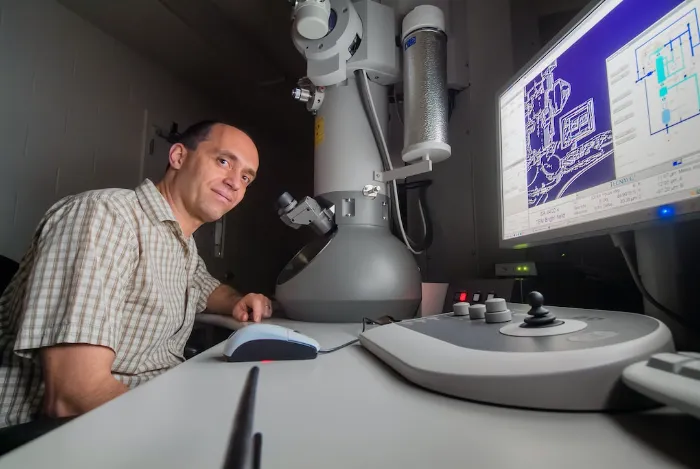
Like a magnifying glass, scanning electron microscopes (SEMs) provide insight into the world of tiny particles. As their name suggests, they are powerful tools used to examine objects at an incredibly small scale and to observe features that would otherwise go unnoticed. They have been around for decades now and remain essential for researchers in many fields such as forensics, materials science, nanotechnology and biology. Here is a glimpse inside the parts of this extraordinary instrument:
1) Electron emitter: The heart of any SEM lies within its electron source which produces electrons through thermionic emission or field emission. Specialized lenses can be adjusted to control the size and shape of the beam generated by these emitters.
2) Scan coils: These electromagnetic coils help move the beam across the surface being scanned. It allows us to adjust how fast we want to look over our sample with high precision so that every detail can be seen clearly.
3) Detectors: At the end of it all, detectors convert the scattered electrons back into signals that can easily be read by computers and analyzed further. Types of detectors range from simple ones like secondary electron detectors to more complex ones like energy dispersive X-ray spectrometers (EDX).
The components mentioned above work together seamlessly allowing scientists to capture detailed images on microscopic scales while revealing new knowledge about what’s going on beneath the surface area. To truly understand how this incredible device works however requires taking a closer look at its operation…
How To Operate A Scanning Electron Microscope
The operation of a scanning electron microscope (SEM) is relatively straightforward but requires some knowledge and training. Using the SEM, users can magnify objects up to one million times their actual size and produce images with very high resolution. To operate an SEM, the user must first select the desired magnification level for their sample. The user then needs to adjust the focus by manipulating the specimen stage. This is done using either manual adjustment knobs or computer-controlled motors depending on the model of SEM being used.
Next, they need to select the type of imaging mode they will use, such as backscattered electrons or secondary electrons. Finally, they should set any parameters specific to that imaging mode such as voltage settings or current levels before collecting data from their sample. Once these steps have been completed, it's time to acquire images from your sample.
To do this, users can move around their sample until they find an area of interest which produces a clear image at low magnification and then switch to higher magnifications when needed. During acquisition, all adjustments are made remotely through a computer interface connected to the SEM itself. It's important to note that no physical contact should be made with the sample during imaging or analysis in order to preserve its integrity and avoid damaging delicate structures within it.
Once acquired, images produced by an SEM can be saved into digital formats for further processing or analysis if needed. From here, users may choose to continue exploring new features on their samples or analyze what has already been collected in more detail – both activities ultimately providing insight into whatever phenomenon was being studied in the first place. Moving forward, let’s now look at some of the advantages and disadvantages of scanning electron microscopy...
Advantages And Disadvantages Of Scanning Electron Microscopy
Scanning electron microscopy (SEM) has been used by scientists since the 1970s and is one of the most powerful tools for studying surface morphology on a nanoscale level. It can magnify objects up to 500,000 times their original size - that's about 200x more than an optical microscope! Its use in scientific research has grown exponentially over the years, with nearly 90 percent of materials science papers now making use of it.
There are many advantages associated with SEM. For example, its high resolution allows for detailed studies on very small samples, enabling researchers to identify intermolecular structures or observe physical changes at the microscopic level. Additionally, because SEM produces images from electrons instead of light like optical microscopes do, they can be used under vacuum conditions and don't require any fluorescent staining agents which may damage fragile samples.
Despite these benefits, there are some drawbacks to using SEM as well. Firstly, due to the complexity of its design and operation costs tend to be quite high compared to other imaging techniques. Secondly, while it offers excellent image resolution when examining two-dimensional surfaces the depth of field is limited so three-dimensional analysis is difficult. Finally, sample preparation before imaging requires specialized knowledge and skill in order to obtain optimal results.
Overall, scanning electron microscopy provides valuable insights into material properties but also comes with certain trade-offs that need to be considered when deciding whether or not this method should be employed for a particular application. From here we'll explore how image analysis techniques can help further enhance our understanding obtained through SEM observations.
Image Analysis Techniques In Scanning Electron Microscopy
Scanning electron microscopy (SEM) is a powerful tool for imaging and analyzing objects on the nanoscale. It produces detailed images of samples that allow researchers to observe features down to the atomic level. An important aspect of SEM analysis is image processing, which involves developing techniques to analyze data collected by this technique. In this article we will discuss some of the major image analysis techniques used in scanning electron microscopy.
One such technique is particle size analysis, which enables us to accurately measure the size distribution of particles within a sample. This type of analysis helps researchers determine if any abnormalities exist in their sample or if there are differences between different groups of particles. Another useful technique is surface topography measurement, which measures the height profile of an object's surface using various methods such as laser interferometry or optical profilometry. This method can be used to identify defects, quantitatively characterize roughness, and estimate mechanical properties.
Another common approach for gathering information from SEM images is automated feature recognition (AFR). AFR utilizes computer algorithms to detect specific patterns or shapes within an image and then quantify them according to predefined criteria. For example, it can be used to count cells or other structures within an image based on shape, color, or intensity characteristics. Additionally, AFR can be used for pattern matching and classification tasks such as identifying materials with similar properties or grouping together similar specimens into categories.
Finally, 3D reconstruction techniques are often employed when studying objects with complex geometries like those found in biological samples. These methods combine multiple 2D images taken at different angles into a single 3D representation that allows researchers to visualize features more clearly than before. By combining these approaches with traditional SEM analysis tools, scientists can gain valuable insight into their samples’ structure and composition at unprecedented levels of detail. With this knowledge they can begin exploring new applications for scanning electron microscopy.
Applications Of Scanning Electron Microscopy
Scanning electron microscopy (SEM) is a powerful imaging technique with many applications. It's used to study the surface of objects at high magnifications, and its ability to capture 3D images has made it especially useful for research purposes. In this article, we'll explore some of the ways SEM can be applied in both scientific studies and industrial settings.
One important use of SEM is material analysis. By providing detailed information about an object's structure and composition, researchers are able to gain insight into how various materials interact with each other or respond to environmental conditions. This includes studying characteristics such as grain size, porosity, corrosion, wear damage, fracture surfaces, and more—all without having to physically remove samples from their original environment.
Another application of SEM is biological research. The technology can provide unprecedented detail on biological specimens down to the cellular level; allowing scientists to observe individual cells within tissues and organs. For example, they may be able to see details such as virus particles or bacterial colonies that were previously too small to identify through traditional imaging techniques.
In addition, SEM also has practical uses in industry where its high resolution capabilities allow manufacturers quality control inspections on products like microelectronic components or medical implants. It provides extremely accurate feedback so producers can quickly identify any defects before shipping goods out for sale—saving them time and money in the long run.
The versatility and usefulness of scanning electron microscopy make it one of the most widely utilized tools in both academic and professional settings today. However, there are certain limitations associated with using the technology which will be discussed next...
Limitations Of Scanning Electron Microscopy
The use of scanning electron microscopy to explore the depths of scientific discovery is a powerful tool. However, as with all tools, it has its limitations. In this section, we will examine these limits and discuss why they can be detrimental to research projects.
It should be noted that even though scanning electron microscopes are incredibly powerful devices for exploring microscopic features at high resolution, their slow operation speeds mean that time-sensitive experiments may have difficulties or become unfeasible when using them. Additionally, some materials exhibit sample charging problems due to electrons being released during irradiation by the microscope’s beam which further reduces image quality. Furthermore, large samples cannot always be scanned in one go since SEMs typically require samples to remain inside the chamber while imaging takes place - meaning that extremely large specimens need to be imaged piecemeal over multiple sessions.
Another limitation of SEMs is more abstract in nature; because different operators tend to take different approaches when setting up an experiment on a new instrument, variation between data sets can arise if not enough attention is paid to how results were obtained. This problem becomes particularly acute when dealing with interdisciplinary teams who don't necessarily understand each other's methods perfectly but are nevertheless trying to draw meaningful conclusions from disparate datasets collected from different instruments operated differently by various people.
Hence, although scanning electron microscopy provides invaluable insights into microstructures across diverse fields such as materials science and life sciences, its inherent limitations must also be taken into account prior to commencing any project involving it so that researchers can manage expectations accordingly and decide whether or not it is suitable for their needs. With proper preparation and consideration of potential issues ahead of time however, scientists can confidently continue leveraging this important technology as a key component of their workflows without fear of running into unexpected obstacles along the way. Now let us move onto safety considerations for using scanning electron microscopy...
Safety Considerations For Using Scanning Electron Microscopy
When working with scanning electron microscopy (SEM), there are safety considerations to take into account. SEM uses a high-energy beam of electrons, which can be hazardous if not used properly. It’s important for users to understand the risks and how to protect themselves from them.
The primary risk associated with using SEM is radiation exposure. The electron beams in SEM have enough energy that when they interact with samples or equipment, they generate x-rays and other forms of radiation. This radiation can cause skin damage, genetic mutations, and even cancer over time if personnel aren't sufficiently shielded or protected. To prevent this kind of harm, operators must use protective clothing like lab coats and gloves as well as face shields and aprons while handling samples and equipment. Additionally, it's essential to limit the amount of time spent near the instrument—especially during operations involving large numbers of electrons.
In addition to protecting against radiation exposure, operators must also minimize their contact with chemicals present in both the sample preparation process and some parts of the machine itself. These substances can include acids or solvents that release toxic vapors into the air, so proper ventilation systems should be installed in labs where SEM is regularly operated. Furthermore, staff should follow all laboratory safety protocols regarding chemical usage and disposal to reduce any potential dangers posed by these materials.
By taking appropriate precautions when operating SEM instruments, researchers can ensure their work environment is safe for everyone involved in its operation. Taking these steps will help create a secure space for research activities without sacrificing productivity or accuracy due to accidents or illnesses caused by negligence towards safety protocols. With careful consideration given to workplace safety measures before beginning experiments with SEM technology, scientists can focus on making progress without worrying about compromising their own health or that of those around them.
Cost Of Scanning Electron Microscopy
Coincidentally, cost is always a factor when it comes to scientific equipment. Scanning electron microscopy (SEM) is no exception - the price of purchasing and maintaining this type of microscope may be overwhelming for some laboratories.
Here are four key points about SEM costs to consider:
1) The upfront purchase price can range from $30,000-$200,000 depending on the model and accessories included.
2) Replacement parts are expensive; even replacing an inexpensive part like a tube lens might set you back several thousand dollars.
3) If you're purchasing used equipment, make sure that it has been thoroughly tested by a qualified technician as repair costs could exceed the original value of the instrument if not done properly.
4) Maintenance contracts are available, but they don't come cheap either - annual fees typically start at around $10k per year and go up from there!
Fortunately, there are ways to save money on your SEM investment. Many vendors offer discounts if multiple systems or upgrades are purchased at once. Additionally, refurbished models tend to be much more affordable than brand new ones - though even with these savings it's important to get them checked out before buying since repairs will still add up quickly if something goes wrong. It's also worth considering renting time on an outside facility instead of buying one outright - in many cases this option can provide greater flexibility while keeping costs down significantly.
In any case, it pays off to do your research ahead of time so you know what kind of financial commitment you'll need to make when investing in an SEM system!
Troubleshooting Tips For Scanning Electron Microscopy
While scanning electron microscopy (SEM) is a powerful tool for imaging the surface of materials at high resolution, troubleshooting SEM can be difficult. It's important to note that even with extensive training and experience, some issues require professional support from qualified technicians. With that being said, here are some tips on how you can improve your own knowledge in order to help diagnose problems with SEM.
First off, familiarizing yourself with the different components of an SEM system will pay dividends when trying to identify which part of the system could be malfunctioning. Knowing where specific parts are located, such as the column, condenser lens, detector chamber or sample stage motors makes it easier to assess what might have gone wrong and narrow down potential solutions.
Secondly, it helps if you understand typical workflows so you can determine whether any steps have been skipped or not done correctly — this may include making sure the right filters have been applied during image acquisition or ensuring proper specimen preparation before imaging begins. Additionally, keeping records of manual operations and settings adjustments allows you to go back and review them more efficiently should similar problems arise again in future experiments.
Finally, by becoming knowledgeable about common sources of errors like beam defocusing or charging artifacts ahead of time — taking into account factors like environmental conditions —can greatly reduce the amount of debugging needed during an experiment session. This also applies to understanding how various parameters affect image quality; doing so facilitates quicker problem-solving no matter what type of material needs to be imaged.
With these basics covered then one can begin exploring future developments in scanning electron microscopy without having wasted too much time troubleshooting simple mistakes or misconfigurations along the way.
Future Developments In Scanning Electron Microscopy
The scanning electron microscope (SEM) has revolutionized the field of microscopy by offering a higher resolution than traditional optical microscopes. But what does the future hold for this incredible tool? From novel imaging techniques to enhanced automation, here's an exploration of some emerging developments in SEM technology.
One advancement is the development of environmental scanning electron microscopy (ESEM). Unlike conventional SEMs that require samples to be placed inside a vacuum chamber, ESEMS can operate at atmospheric pressures and can even image wet or living specimens without damage. This opens up possibilities like direct monitoring of microorganism growth, as well as real-time observation of biological processes such as cell migration and tissue formation.
Another improvement being worked on is automated sample processing with robotic loading systems. These robots improve efficiency by automatically transferring samples from one place to another, eliminating manual handling errors and drastically reducing turnaround time between experiments. Additionally, they have been used to automate complex protocols such as fixing multiple biological samples onto grids before imaging them in the SEM chamber.
Finally, researchers are working on new methods to enhance contrast in images taken with an SEM. One approach involves coating gold nanoparticles onto cells or tissues prior to imaging which produces high-contrast images due to light scattering effects caused by the particles' size and shape. This technique could be useful for studying small cellular structures within larger tissue sections or distinguishing different types of viruses based on their surface morphology.
As these examples demonstrate, there are exciting advancements underway in order to make SEM easier, faster and more powerful - all while expanding its applications into previously inaccessible areas!
Frequently Asked Questions
What Is The Resolution Of A Scanning Electron Microscope?
It's like a journey to the furthest depths of science. Scanning electron microscopy (SEM) has taken us further than ever before; we can now observe materials down to the very atomic level. It is truly incredible how far technology has come and what SEM allows us to see.
But with such power comes great responsibility, and so it's important that we know just what this tool is capable of – namely its resolution capabilities. How much detail can be seen in an image produced by a scanning electron microscope?
The answer isn't as simple as one might think, for there are many variables at play that affect resolution. Depending on the type of specimen being viewed, different conditions may require more or less resolution from the microscope itself. Additionally, certain types of detectors used in the process also have an effect on sharpness and clarity. In general terms though, resolutions up to 0.5 nanometers (nm) can usually be achieved when using modern equipment.
In short, SEM gives scientists powerful insight into material structures which was previously impossible to achieve without taking samples away from their original environments; these images provide invaluable data regarding composition and behavior of natural specimens or manufactured products alike. We owe our current understanding of microscopic phenomena largely thanks to scanning electron microscopes' remarkable ability to give us a window into worlds unseen by human eyes before now.
How Long Does It Take To Prepare A Sample For Scanning Electron Microscopy?
The world of microscopy is full of wonders, and scanning electron microscopy (SEM) stands out as one of the most powerful tools available to scientists. But a successful SEM experiment requires much more than just turning on the machine – it takes careful preparation. So how long does it take to prepare a sample for SEM?
The answer depends largely upon the type of sample being used and the complexity of its structure. For instance, if you're working with something like an insect's exoskeleton, which has already been dried or preserved in some way, then preparation time might be minimal; but if you need to create a thin section from a larger piece of material, such as rock or metal alloy, then that could take several hours before any imaging can begin.
In either case, though, there are certain steps that must always be taken prior to using an SEM device: cleaning away impurities from the surface of the specimen so that they don't interfere with image quality; coating the object with conductive material so that electrons will flow freely during imaging; and finally making sure all parts are securely mounted in order for accurate results. All these tasks require skill and precision – hence why experienced technicians often have years of experience under their belt when it comes to preparing samples for SEM work.
What this means is that while modern technology may make it possible to carry out complex experiments quickly and efficiently, no amount of technological advancement can replace human knowledge and expertise when it comes to ensuring success in scientific research endeavors. Preparing specimens correctly is crucial for obtaining reliable data – no matter what kind of microscope we use!
Is It Necessary To Wear Protective Gear While Using A Scanning Electron Microscope?
The scanning electron microscope is an intricate and powerful tool that has opened up a world of microscopic exploration. It's like peering through the keyhole into a realm filled with secrets, where answers to some of life’s most fascinating questions can be found. But as with all scientific instruments, safety precautions must be taken when working with them - which brings us to our question: Is it necessary to wear protective gear while using a scanning electron microscope?
Symbolically speaking, protecting ourselves from harm is analogous to putting on layers of armor for battle. In this case, we are equipping ourselves against the invisible dangers associated with handling these sensitive machines. The answer is yes; protective gear should always be worn while operating a scanning electron microscope in order to minimize potential risks such as exposure to radiation or electric shock. Depending on what type of sample is being examined, additional protection may be required (e.g., rubber gloves).
When dealing with hazardous materials or environments, there can never be too much caution exercised - especially when one considers the long-term health effects of neglecting proper safety protocols. Protective clothing not only safeguards researchers but also helps protect equipment by reducing dust particles and other contaminants from entering the system; thus preventing damage and ensuring reliable performance over time.
Therefore, wearing appropriate gear while utilizing a scanning electron microscope is essential in order to maintain optimal user safety and ensure maximum longevity of the machine itself. With cautiousness comes peace of mind knowing that any discoveries made will not come at the cost of one’s wellbeing.
Is There A Difference In Cost Between Different Types Of Scanning Electron Microscopes?
Have you ever wondered what the cost difference might be between different types of scanning electron microscopes? It's a valid question to consider, as these instruments are essential for certain scientific applications. Scanning electron microscopy (SEM) has become an integral part of everyday life and is used in many industrial areas such as manufacturing processes and quality control.
The cost differences between SEMs come down to several factors, including type of instrument and the level of sophistication needed. For example, basic models can range from around $50,000 to more than one million dollars depending on features like depth resolution, high-resolution imaging capabilities, digital interface modules and other advanced functions. More complex systems may also require additional installation costs for specialized technical support personnel or software upgrades.
Another factor that impacts the price tag associated with SEMs is the availability of related services. Maintenance contracts and training programs often carry extra charges beyond just purchasing the equipment itself. On top of this there are also potential labor expenses if users decide to hire staff specifically trained in operating the microscope correctly.
When it comes to choosing which type of SEM best suits your needs, it’s important to take into consideration all available options before making a purchase decision. Ask yourself questions like: How much space do I have for installing? What kind of samples will I be analyzing? Do I need any special features included in my system? By considering all aspects carefully you’ll be able to make an informed choice about which model will work best for you without breaking the bank! TIP: Talk to people who already have experience using similar microscopes so they can provide firsthand insight into their own experiences when selecting a specific model.
Are There Any Special Maintenance Requirements For Scanning Electron Microscopes?
When looking into scanning electron microscopes (SEMs), it's important to consider the maintenance requirements. Proper upkeep is essential for maintaining SEM performance and accuracy. It can also be beneficial in terms of cost, since preventive maintenance reduces repair costs later on.
The main thing to keep an eye out for is component integrity. SEMs contain delicate parts that must stay clean and intact to function correctly. Regularly inspect all components for signs of wear or damage such as scratches, chips, cracks, etc. A trained technician should handle any necessary repairs or replacements.
In addition, dust particles can easily accumulate inside a SEM environment due to static charge buildup and air circulation patterns within the chamber. Clean the interior using compressed air or other approved methods when needed. This will help prevent operational problems caused by dirt build-up over time.
Other than these general guidelines, specific maintenance requirements depend largely on the type of SEM being used and its application in the lab setting. Consult with your supplier/manufacturer if you need further information about how best to maintain your particular model or system setup. TIP: In line with proper maintenance practices, always remember to use safety equipment like gloves, goggles and masks whenever handling a microscope’s inner workings!
Conclusion
Scanning electron microscopy is a powerful tool for examining the nanoscale features of materials. With its high resolution and relatively fast imaging times, it has become an indispensable technique in research laboratories across the world. It also requires special maintenance considerations and protective gear to ensure safe operation, as well as more expensive models that offer higher resolutions than standard microscopes.
Although scanning electron microscopy may appear complex at first glance, it is actually quite straightforward once all of its components are understood. Just like a puzzle with many pieces hidden beneath the surface, learning how to use this technology allows scientists to piece together images from tiny parts and gain valuable insight into their samples.
In short, scanning electron microscopy provides researchers with an invaluable window into the microscopic realm – one that can open up entirely new realms of knowledge if used correctly. So whether you’re using it to analyze microbes or map out molecules, think of your Scanning Electron Microscope as a magical microscope capable of uncovering entire worlds on a miniscule scale.